Example part: CP2108
Datasheet: https://www.silabs.com/documents/public/data-sheets/cp2108-datasheet.pdf
Create a new unit
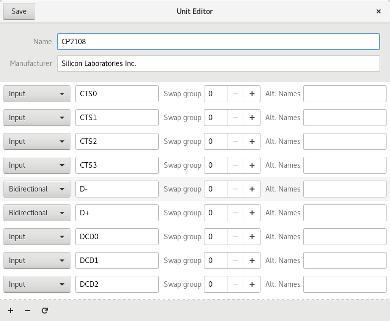
This seems to be about transferring the pin names and descriptions from the datasheet into Horizon. I filled in the entries based on table 4.1: Pin Definitions for CP2108 QFN64 from the datasheet.
- Go to the ‘Units’ tab
- Click create and enter the part name and manufacturer
- Click the ‘+’ in the bottom left to start entering pins
- Note: you do not have to add pins multiple times if they are logically the same. Eg., only one VIO is required even if this particular package for the CP2108 has multiple pads for it.
- Non-Connected pins (NCs) and QFN central pads probably should not be added unless they contribute the logical connections required for the unit.
A few notes about this interface:
- The interface is best suited to entering data by numbering order eg. CTS0, CTS1, …, CTSn
- Use the pin’s primary function as their name. It’s tempting to use the pin numbers; however, that seems to make it difficult to create the symbol for the unit in the next step.
- The alternate name section adds a trailing space when adding new rows
After saving, the pool will update and your unit will be in the list. This is one of the most rote processes in adding parts to Horizon.
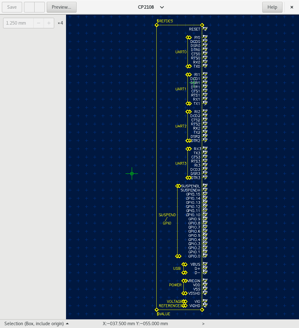
Create a new symbol
The symbol seems to be used to represent a slightly abstracted ‘block diagram’ of the part. I’m not sure if it’s convention, but the parts in the Horizon example pool are rectangular with all pins on the right. I recommend following this convention. As the basis for the symbol in the case of the CP2108, I have followed the block diagram presented on the first page (alternatively, the figures in section 6 seem to be good as well).
- Go to the ‘Symbols’ tab
- Click create and enter the part name (‘CP2108’)
- Choose a new file and folder into which to save the symbol json file
- Enter ’d L’ and draw a new rectangle.
- For each pin out:
- Using ‘p p’, add a pin: select the pin by number (it’s useful to have the unit reference or datasheet open for this)
- Pins auto-increment by pin number for placement, so if pins follow each logically it is quite quick to place many of them.
- For each logical group of pins, use ’d l’ to draw a small open-sided rectangle around the pins in the group, and place a descriptor using ‘p t’
- Note: rectangle lines can be clicked on, then dragged, in order to reshape the symbol shape as necessary.
- Using ‘p t’, add two text items: ‘$REFDES’ and ‘$VALUE’ text elements to the symbol. These are typically on the top-left and bottom-left respectively. Placement may vary for non-IC parts.
Create a new entity
Entities are the logical presentation of the part in schematic. I believe they are analogous to block diagrams in datasheets.
There are several block diagrams presented in the datasheet, but I used the one on the first page as a basis for this entity.
- Update the pool by clicking ‘Update pool’ in the top left
- Open the ‘Entities’ tab
- Click the ‘Create’ button
- Enter the part information:
- Name: CP2108
- Manufacturer: Silicon Laboratories Inc.
- leave “Prefix” empty
- Tags: ic controller
- Click the ‘+’ symbol in the bottom-left and choose a unit to add to the entity. @TODO: No idea what to put in the different fields. No explanation is provided.
- Click save (top left) save choose a location. Eg. ic/controller/slab/cp2108.json
- Close out the edit window and let the pool update
Create a new package
Packages are the details of the physical assemblies. The default pool has a number of packages available, including generic options for common types; however, these will probably not fit the bill for the part you have chosen.
For the CP2018, I used pages 16-18 to the rev 1.2 datasheet as reference for the dimensions of the package and recommended PCB layout.
Pads and pins
In the case of this part, the default pool has examples of QFN packages for 17 and 33 pins, but not the larger 64 pins used in the CP2108. Furthermore, the generic packages have different patch pitch and dimensions.
First, in the pool manager’s packages tab, add a new package for the part. In this example I will create the package as a generic QFP-64 package, but it’s probably more appropriate to create a new vendor specific package. The new package interface will create a folder into which the the package files will be saved. The folder name should be a slug for the package, eg. qfn-64.
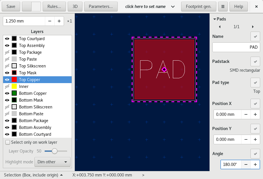
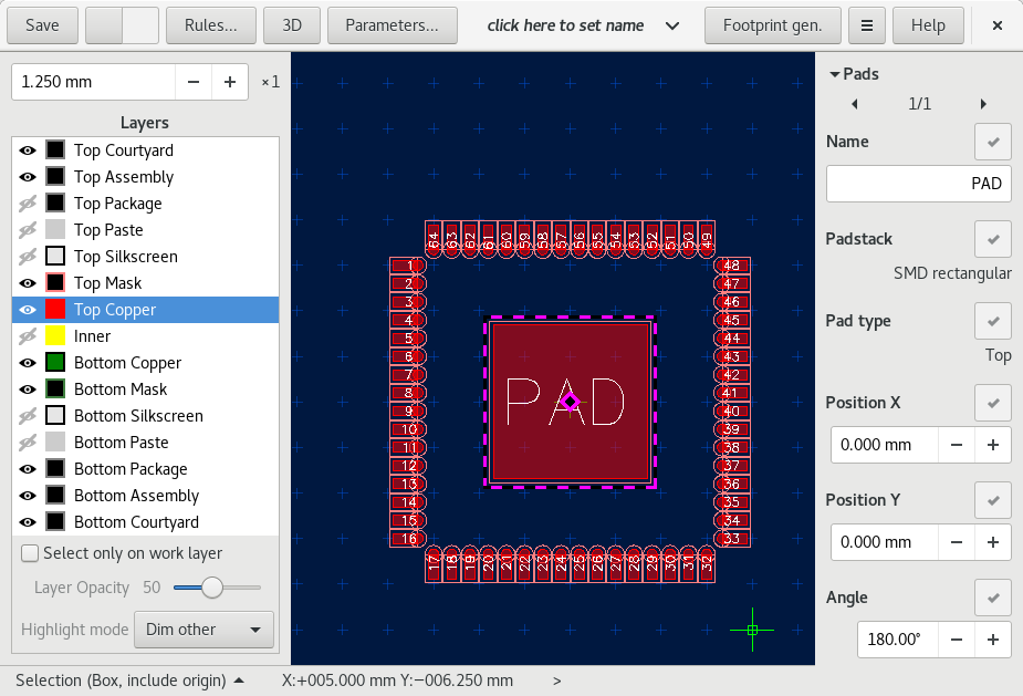
Once it’s created, a new schematic editor window should be opened. Here, we’ll start with the footprint layout using avaiable generator. We’ll create the centre pad first: it’s a single type pad with a rectangular footprint (or padstack in Horizon’s parlance). From the datasheet we can use the X2 and Y2 dimensions for the pad and the pitch may be ignored as it’s a single pad. The pad should appear once you hit generate and you can click on it to change the name from ‘1’ to ‘PAD’.
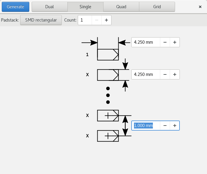
The process to generate the 64 pads from in quad form is similar: the padstack is a rectangular oblong padstack in a 16 x 16 configuration. The values from the datasheet can be easily entered - the only deviation is that Horizon uses C1/2 and C2/2 instead of C1 and C2 respectively. The new pads will be numbered sequentially starting from the top-left and ascending in a counter-clockwise direction.

By this point the top copper, mask, and paste layers should be filled in automatically. For this part, I think it’s good enough. The next step of data entry is to add in the top package (the physical package dimensions), the top assembly (approximation of the parts shape and definining features), and courtyard (space to leave around to assembly).
Top Package
We’ll start with the ‘Top Package’. This is meant to be the physical package dimensions, while the following section (Top Assembly) is a more symbolic layout.
- Select the ‘Top Package’ layer
- In the case of the CP2108, the physical package has cut corners with a width of L (0.3mm - 0.5mm with a typical width of 0.4mm). Set the marker spacing in the top-left to the minimum distance you want to represent. In this case, I chose 0.5mm and zoomed in until the markers were represented 1x on the screen.
- The tools, perhaps counter-intuitively, are typically only accessible via keyboard shortcuts. To start drawing a polygon, hit ’d y’ on the keyboard then click the starting point. Place each vertex then hit ‘Escape’ to finish.
Top Assembly
Repeat the process ‘Top Package’ for the ‘Top Assembly’ layer, but the shape may be simpler. If your top assembly is simply rectangular, it’s easier to use ’d Y’ to do the drawing. The assembly layer should include a visual indication of the first pin’s location, a single cut corner is often used.
Specifically, my approach is to do the following:
- Type ’d Y’ to start drawing a polygon rectangle.
- Click on the centre point of the package
- Click a corner vertex at the appropriate position
- Type ’d’ to cycle through the decorations to add an indicator for the first pin
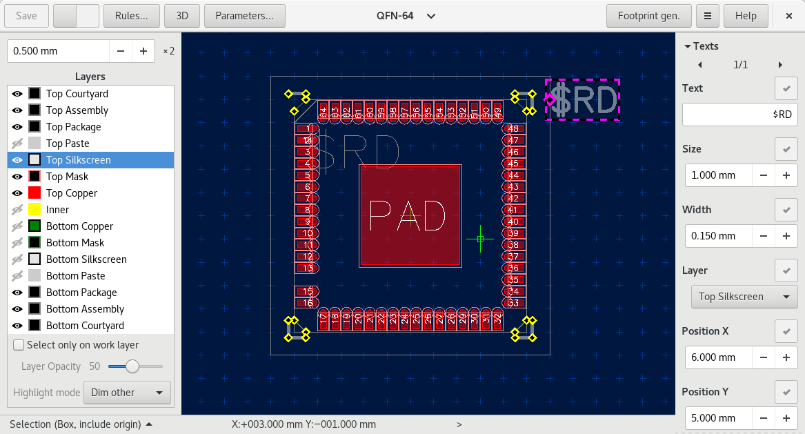
Place a stub for the part identifier. Hit ‘p t’ on the keyboard, enter the stub “$RD”. Resize the text so that “$RD4444” still fits within the polygon. Place the text near the first pin.
Top Courtyard
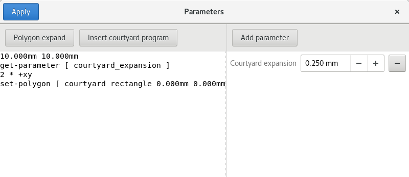
Finally, for the ‘Top Courtyard’ the best approach seems to be to add it using a small bit of script.
- Select the ‘Top Courtyard’ layer
- Use ’d Y’ to start drawing a new vertex rectangle
- Click a starting vertex in the corner
- @TODO: Confirm that the starting corner should be on the edge of the outer leads.
- In the case of complicated parts, you may need to use polygons
- Hit ‘c’ to enter corner mode
- Select the ending vertex
- Using Ctrl-LMB, select the 4 edges of the newly created polygon
- In the preferences panel, enter the class ‘courtyard’ and hit enter.
- Open the parameters window by clicking on the button in the top of the window
- Add a new parameter, ‘Courtyard expansion’
- Click the button ‘Insert courtyard program’
- Modify the size in the left hand box (first line) to match the package size.
In this case, I used
10.000 mm 10.000 mm
Silkscreen
The silkscreen layer is used to print information on to the boards for reference. There are three important features to add:
- Part placement guides
- An indication of where the first pin is (unless the part isn’t orientation sensitive)
- Place an placeholder for the part number
For the CP2108, here’s what I did:
- Select the ‘Top Silkscreen’ layer
- Switch the grid to 0.100 mm
- For each corner, zoom in until you ther grid markers are 1x
- Start drawing a line by typing ’d l’ and clicking on point
- Press ‘w’ and set the width to 0.150 mm
- Create an ‘L’-shaped corner ~0.200 mm from the corners of the footprint
- Hit escape to finish drawing
I then modified the top-left corner and cut one of the segments to indicate the first-pin position.
Finally, placing the part number placeholder:
- ‘p t’ to select the place text tool
- Choose a point ~0.150 mm from the top right corner of the pad
- Enter the text “$RD” and hit enter to finish
- Select the placed text and change the size to 1.000 mm and width to 0.15 mm
Wrap-up
Save that package!
Note, there is an option to import from DXF files. I tried this and didn’t achieve the results I was expecting. Even if it works, not all manufacturers may provide these openly from what I can see.
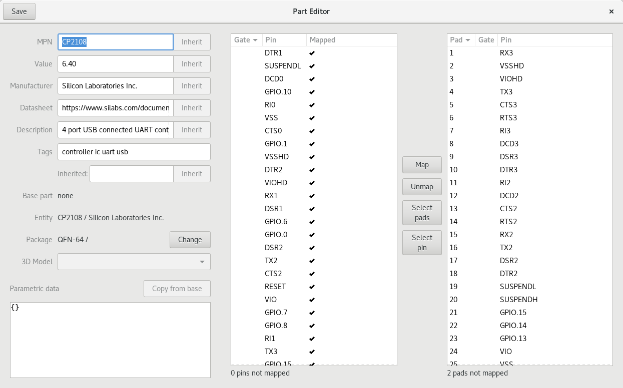
Create a new part
- Open the parts tab and start a new part by click on create.
- Select the entity and the package for the part, then choose where to save it.
- If you don’t see any pins to map to pads, make sure the entity has a unit assigned to it.
- Start mapping the pins to the pads in the package.
- Use Ctrl-click to select multiple pads for a given before hitting ‘Map’
Notes and caveats
This was written as I was learning. Hopefully this helps folks, but probably has omissions and errors!
License
This post and associated screenshots are licensed under the Creative Commons Attribution-ShareAlike 4.0 International CC BY-SA 4.0